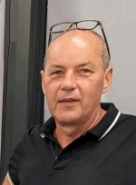
Armin Kriele

Armin Kriele
Neutronenstreuung, Hereon-Außenstelle am FRM II in Garching bei München
IngenieurTel: +49 (0)89 158860-806
• Lab responsible Materials Science Lab
• Environmental Scanning Electron Microscopy (ESEM)
• Energy Dispersive X-ray Spectroscopy (EDS)
• Alloys, ceramics/minerals, batteries, fuel cells, soft matter
Armin Kriele is a physics engineer with extensive experience in the areas of sample preparation and analytics. This includes the complete process chain in the production of quantum nano dots and nanomechanical devices from IV and III-V semiconductors, as well as the production of CVD nano diamond for MEMS/NEMS bio sensors.
Armin is very experienced in micro- and nanoanalytics such as single molecule SPM, STM, electron microscopy (SEM, ESEM), energy dispersive x-ray spectroscopy and XRD on all types of samples.
He holds several patents in the field of manufacturing SPM sensors and in-situ temperature control devices for XRD analysis on batteries.
Website – a private one which is not related to science but to my activities in arts
Professional and industry experience
since 2012 Helmoltz-Zentrum Geesthacht, GEMS German Engineering Materials Science Center at outstanding MLZ Garching
• Technical Manager of Material Science Lab (Hard- and Soft Matter)
• Environmental Scanning Electronmicroscopy (ESEM) and EDS analysis
• Micro structure analysis by XRD, DSC, AFM and SAXS (ceramics, battery materials, alloys, nanoparticle suspensions, biomaterials, thin films etc.)
• Metallographic sample preparation
2011-2012 Heinz Meier-Leibnitz Neutron Research Center MLZ, Neutronoptics
• Development of new neutron guides
• PVD coating of neutron super mirrors
• AFM, XRD, SEM Analytics
2006-2011 Fraunhofer Institute for Applied Solid State Physics IAF Freiburg, Departement Micro- and Nanosensors, CVD Diamond Group
• Manager of Bio-electrochemistry and AFM analytic Lab
• Equipment acquisition of JPK Nanowizzard III, Veeco Nanoscope III, Nanosurf easyscan 2, Wyco white light interferometer
• Micro-mechanical investigations on nano diamond thin films and membranes
• Development of MEMS/NEMS for bio sensors
• Protein and DNA characterisation
• Responsible for the Quality Management of the Department
2002-2005 NanoTOOLS GmbH München; sensors for scanning probe microscopy
• Manager, shareholder and founder (1996)
• Development and mass production of high aspect ratio AFM scanning probes for semiconductor industry
• Responsible for R&D, product placement, international cooperations
1995–2002 LMU-München, Sektion Physik, Lehrstuhl Festkörperphysik Prof. Dr. J.P. Kotthaus
• Manager of the cleanroom laboratory
• responsible for acquisition and installation of large process- and manufacturing tools
• Process development for IV and III-V semiconductors.
1992–1994 GSF Forschungszentrum für Umwelt und Gesundheit, Helmholtz Zentrum, Neuherberg
• Risk analysis for II-VI thin film photovoltaic solar cells (CdTe, CIS)
• Element analysis with ICP atom emission spectroscopy
 journal articleStructural response of silicon-containing graphite anodes on lithium intercalationHölderle, Tobias,Petz, Dominik,Kochetov, Vladislav,Baran, Volodymyr,Kriele, Armin,Hegedüs, Zoltán,Lienert, Ulrich,Avdeev, Maxim,Müller-Buschbaum, Peter,Senyshyn, Anatoliy (2025)
In: Energy Storage Materials, Vol. 75, 104042, Elsevier, Amsterdam. journal articleCharacterizing effects of hydrogen ingress in Ti–Mg based hybrid implant materialsKumar, Richi,Solís, Cecilia,Trtik, Pavel,Kriele, Armin,Limberg, Wolfgang,Wieland, D.C. Florian,Moosmann, Julian,Serdechnova, Maria,Blawert, Carsten,Ebel, Thomas,Willumeit-Römer, Regine,Garamus, Vasil M. (2025)
In: RSC Advances, Vol. 15, 6, 4472-4480, Royal Society of Chemistry, London. journal articleNanoparticle-encapsulated organo-magnetogels: crosslinked network for broad-spectrum pollutant removalSridhar, Sanjeevi Prasath,Uthaman, Sudha,Pandurangan, Logesh Kumar,Kriele, Armin,Saha, Debasish,Wu, Baohu,Parthiban, Velraj,Murugesan, Janaki Vembu,Vijayakumar, Balachandar,Förster, Stephan,Radulescu, Aurel,Joseph, Brijitta (2025)
In: npj Clean Water, Vol. 8, 1, 66, Springer Nature, Basingstoke. journal articleCooperative gelation of syndiotactic polystyrene and low molecular weight PEGDMERadulescu, Aurel,Joseph, Brijitta,Han, Zehua,Kriele, Armin,Lamparelli, David Hermann,Allgaier, Jürgen,Cheng, He (2025)
In: Macromolecular Materials and Engineering, -e00126-, Wiley, Weinheim.
